Metasurface Integrated Microbolometers
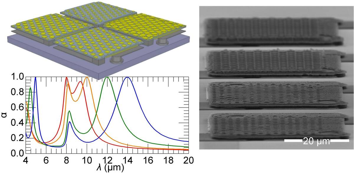
Infrared sensing allows imaging of the heat emitted by objects. Microbolometers are widely used for uncooled imaging. These sensors are typically optimized for the transparent region of the atmosphere (8-14 µm) but can be scaled throughout the infrared. Incident radiation is converted to heat by the microbolometer, raising the temperature of the pixel which changes its electrical resistance. The electrical resistance is measured. The sensitivity, speed, and noise of a microbolometer are functions of the pixel material properties. Our research is focused on integrating metasurfaces with the microbolometer sensing layer (typically a semiconductor). The metasurface determines the absorptance of the pixel and allows its wavelength and polarization response to be engineered pixel-to-pixel by varying only the geometry. The array of metal/semiconductor junctions also affects the electrical performance of the microbolometer, lowering its resistivity and increasing the magnitude of the temperature coefficient of resistance. The design of the metasurface also affects the thermal mass as well as the cost (tied to feature size) of the microbolometer. Understanding these relationships and the interdependence with the semiconductor sensing layer, in-short considering the pixel as a metamaterial with geometry dependent optical, electrical and thermal properties, has the potential to lead to improvements in overall performance as well as new low-cost high performance multispectral imagers.